- 您现在的位置:买卖IC网 > Sheet目录515 > SIR462DP-T1-GE3 (Vishay Siliconix)MOSFET N-CH 30V 30A PPAK 8SOIC
�� �
�
�SiR462DP�
�Vishay� Siliconix�
�N-Channel� 30-V� (D-S)� MOSFET�
�PRODUCT� SUMMARY�
�V� DS� (V)� R� DS(on)� (� Ω� )�
�I� D� (A)�
�Q� g� (Typ.)�
�FEATURES�
�?� Halogen-free� According� to� IEC� 61249-2-21�
�?� TrenchFET� ?� Power� MOSFET�
�30�
�0.0079� at� V� GS� =� 10� V�
�0.010� at� V� GS� =� 4.5� V�
�30� a�
�30� a�
�8.8� nC�
�?� 100� %� R� g� Tested�
�?� 100� %� UIS� Tested�
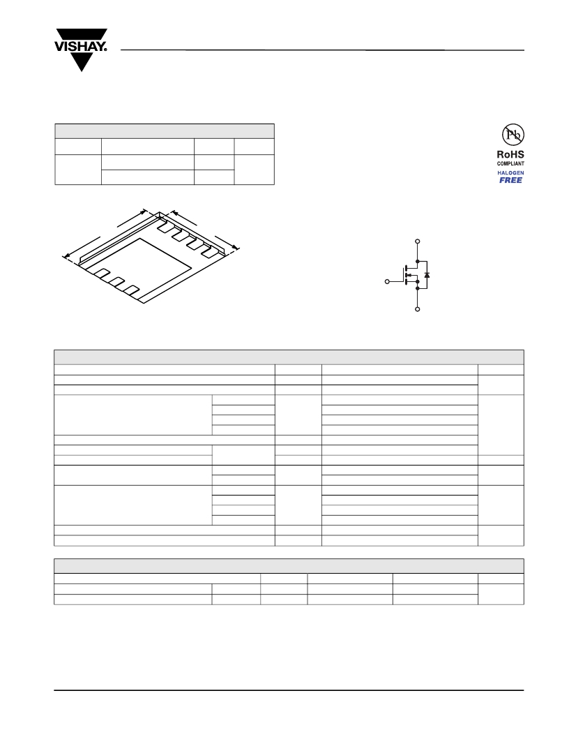
�PowerPAK� SO-8�
�APPLICATIONS�
�?� High-Side� Switch�
�?� Server,� VRM,� POL�
�6.15� mm�
�1�
�S�
�S�
�5.15� mm�
�?� DC/DC�
�D�
�2�
�3�
�S�
�G�
�4�
�D�
�8�
�7�
�D�
�D�
�G�
�6�
�5�
�D�
�Bottom� View�
�Ordering� Information:� SiR462DP-T1-GE3� (Lead� (Pb)-free� and� Halogen-free)�
�ABSOLUTE� MAXIMUM� RATINGS� T� A� =� 25� °C,� unless� otherwise� noted�
�S�
�N� -Channel� MOSFET�
�Parameter�
�Drain-Source� Voltage�
�Gate-Source� Voltage�
�T� C� =� 25� °C�
�Symbol�
�V� DS�
�V� GS�
�Limit�
�30�
�±� 20�
�30� a�
�Unit�
�V�
�Continuous� Drain� Current� (T� J� =� 150� °C)�
�Pulsed� Drain� Current�
�Avalanche� Current�
�Avalanche� Energy�
�Continuous� Source-Drain� Diode� Current�
�T� C� =� 70� °C�
�T� A� =� 25� °C�
�T� A� =� 70� °C�
�L� =� 0.1� mH�
�T� C� =� 25� °C�
�T� A� =� 25� °C�
�I� D�
�I� DM�
�I� AS�
�E� AS�
�I� S�
�30� a�
�18.9� b,� c�
�15.1� b,� c�
�70�
�31�
�48�
�30� a�
�4� b,� c�
�A�
�mJ�
�A�
�T� C� =� 25� °C�
�41.7�
�Maximum� Power� Dissipation�
�T� C� =� 70� °C�
�T� A� =� 25� °C�
�P� D�
�26.7�
�4.8� b,� c�
�W�
�T� A� =� 70� °C�
�3.1� b,� c�
�Operating� Junction� and� Storage� Temperature� Range�
�Soldering� Recommendations� (Peak� Temperature)� d,� e�
�T� J� ,� T� stg�
�-� 55� to� 150�
�260�
�°C�
�THERMAL� RESISTANCE� RATINGS�
�Parameter�
�Symbol�
�Typical�
�Maximum�
�Unit�
�Maximum� Junction-to-Ambient� b,� f�
�Maximum� Junction-to-Case� (Drain)�
�t� ≤� 10� s�
�Steady� State�
�R� thJA�
�R� thJC�
�21�
�2.4�
�26�
�3.0�
�°C/W�
�Notes:�
�a.� Based� on� T� C� =� 25� °C.� Package� limited.�
�b.� Surface� Mounted� on� 1"� x� 1"� FR4� board.�
�c.� t� =� 10� s.�
�d.� See� Solder� Profile� (� http://www.vishay.com/ppg?73257� ).� The� PowerPAK� SO-8� is� a� leadless� package.� The� end� of� the� lead� terminal� is� exposed�
�copper� (not� plated)� as� a� result� of� the� singulation� process� in� manufacturing.� A� solder� fillet� at� the� exposed� copper� tip� cannot� be� guaranteed�
�and� is� not� required� to� ensure� adequate� bottom� side� solder� interconnection.�
�e.� Rework� Conditions:� manual� soldering� with� a� soldering� iron� is� not� recommended� for� leadless� components.�
�f.� Maximum� under� Steady� State� conditions� is� 70� °C/W.�
�Document� Number:� 68823�
�S-82771-Rev.� C,� 17-Nov-08�
�www.vishay.com�
�1�
�发布紧急采购,3分钟左右您将得到回复。
相关PDF资料
SIR464DP-T1-GE3
MOSFET N-CH 30V 50A PPAK 8SOIC
SIR468DP-T1-GE3
MOSFET N-CH 30V 40A PPAK 8SOIC
SIR470DP-T1-GE3
MOSFET N-CH 40V 60A PPAK 8SOIC
SIR472DP-T1-GE3
MOSFET N-CH 30V 20A PPAK 8SOIC
SIR474DP-T1-GE3
MOSFET N-CH D-S 30V PPAK 8SOIC
SIR494DP-T1-GE3
MOSFET N-CH D-S 12V PPAK 8SOIC
SIR67-21C/TR8
LED IR TOP FLAT WATER CLEAR SMD
SIR698DP-T1-GE3
MOSFET N-CHAN 100V(D-S)POWERPAK
相关代理商/技术参数
SIR462DP-T1-GE3
制造商:Vishay Siliconix 功能描述:N CHANNEL MOSFET 30V 30A SOIC 制造商:Vishay Siliconix 功能描述:N CHANNEL MOSFET, 30V, 30A, SOIC
SIR464DP
制造商:VISHAY 制造商全称:Vishay Siliconix 功能描述:N-Channel 30-V (D-S) MOSFET
SIR464DP-T1-GE3
功能描述:MOSFET 30V 50A 69W 3.1mohm @ 10V RoHS:否 制造商:STMicroelectronics 晶体管极性:N-Channel 汲极/源极击穿电压:650 V 闸/源击穿电压:25 V 漏极连续电流:130 A 电阻汲极/源极 RDS(导通):0.014 Ohms 配置:Single 最大工作温度: 安装风格:Through Hole 封装 / 箱体:Max247 封装:Tube
SIR466DP
制造商:VISHAY 制造商全称:Vishay Siliconix 功能描述:N-Channel 30-V (D-S) MOSFET
SIR466DP-T1-GE3
功能描述:MOSFET 30V 40A 54W 3.5mohm @ 10V RoHS:否 制造商:STMicroelectronics 晶体管极性:N-Channel 汲极/源极击穿电压:650 V 闸/源击穿电压:25 V 漏极连续电流:130 A 电阻汲极/源极 RDS(导通):0.014 Ohms 配置:Single 最大工作温度: 安装风格:Through Hole 封装 / 箱体:Max247 封装:Tube
SIR468DP
制造商:VISHAY 制造商全称:Vishay Siliconix 功能描述:N-Channel 30-V (D-S) MOSFET
SIR468DP-T1-GE3
功能描述:MOSFET 30V 40A 50W 5.7mohm @ 10V RoHS:否 制造商:STMicroelectronics 晶体管极性:N-Channel 汲极/源极击穿电压:650 V 闸/源击穿电压:25 V 漏极连续电流:130 A 电阻汲极/源极 RDS(导通):0.014 Ohms 配置:Single 最大工作温度: 安装风格:Through Hole 封装 / 箱体:Max247 封装:Tube
SIR470DP
制造商:VISHAY 制造商全称:Vishay Siliconix 功能描述:N-Channel 40-V (D-S) MOSFET